CRYPTON Hardware Implementation
by Nguyen Nguyen
  1. Overview
  2. CRYPTON is selected to be a candidate for the future Advance Encryption Standard (AES) due to its high level of security, feasible implementation, and high performance. The algorithm was provided in software in both C and Java codes. In the project, a hardware implementation of the algorithm is considered. This specification provides the guidelines to implement CRYPTON in hardware, and outlines the performance of the algorithm in Field Programmable Gate Arrays (FPGA). Due to the space limitation of the device space, twelve-round scheme will not be used. Instead, the focus will be on two-round implementation. If time allows, the number of rounds in the implementation may be increased. The specification contains the following sections:


    Section 1 discusses the overview of this documentation

    Section 2 lists references and relevant documentation

    Section 3 discusses the functions and the and the architecture of the design

    Section 4 describes the design methodology to be used

    Section 5 outlines the procedure for testing the functionality and performance of the design

    Section 6 discusses the areas that may be changed depending on the project progress

    Section 7 lists the schedule of tasks to carry the project


  3. Reference
  4. Lim, Chae. “Specification and Analysis of CRYPTON”, Version 1.0. December 1998.
     

  5. Functions and Architecture
  6. The circuit consists three main functional blocks. These are Encryption/Decryption, Key Schedule, and Inbound Controller. The Encryption/Decryption block will perform both encryption and decryption. The scheme for both encryption and decryption will be identical, but the key scheduling is different in one process from the other. Key Schedule is an important process in the CRYPTON algorithm, and has to work in synchronization with both encryption and decryption. The Key Schedule will be responsible for scheduling the keys properly for each mode encryption or decryption. The Inbound Controller will provide synchronization between Key Schedule and Encryption/Decryption blocks. Figure 1 shows the block diagram of the CRYPTON design.
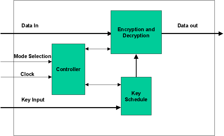


    Figure 1 - Block Diagram of The CRYPTON Circuit
     
    1. Key Schedule
    2. Key Schedule will take in 256-bit user key, and schedule the keys for all rounds of encryption and decryption The key scheduling mechanisms for encryption will be different from the decryption. The 256-bit user key is fed to the Key Schedule block serially. This block will implement the algorithm of key schedule as specified in reference (1). Detailed design of this block will be provided later as an appendix in the final report.
       

    3. Encryption/Decryption
    4. The design will adhere to the encryption/decryption algorithm CRYPTON. In the encryption mode, this block will accept a 128-bit block message and produce a 128-bit block cipher text. In the decryption process, the cipher-text is fed in as the input and the deciphered message is produced on the output side. The encryption and decryption processes are identical in this block, and the Key Schedule block will provide proper keys to carry out the operation. Detailed design of the block is still to be defined.
       

    5. Controller
    The Controller block will provide the synchronization of between the Key Schedule block and the Encryption/Decryption block. It also allows the user to select the cryptographic mode (encryption/decryption). The Controller will provide the clock to the other two blocks.
     
  7. Design Methodology
  8. The design will mainly use VHDL to implement to algorithm. Schematic capture option may be used at the top level to show main functions of the design. Xilinx will be the target of the implementation, but depending on the number of configuration logic blocks used (CLB), the specific device will be chosen. At this time, Xilinx XL4013E will be the candidate target of the implementation. Please note that the tool selection will be determined by the availability of the tools and our accessibility. Further information of the design methodology is listed in Table 1.


    Design Entry Mainly VHDL; schematic may be used at top level; Logic Blox may be used
    CAD Tools Synario and/or Xilinx Foundation Series
    Simulation Aldec Evaluation version 3.3 or Model Tech
    Device XC4013E, or maybe a bigger device
    Synthesizer Metamor, or Cadence
    Table 1 – Design Methodology
     
  9. Design Verification and Evaluation
The design verification and evaluation consist of the following main procedures:
    1. Functional Simulation
    2. Functional simulation to be done on the circuit design will be a VHDL testbench. The test bench will have the capability to convert a text message into binary bits, and then select the proper mode to operate the circuit. The testbench also provides binary bit to text conversion, which makes the decryption process easy to verify. Both encryption and decryption will be simulated. Deciphered text will be compared against the plain text.


      Besides verifying the data in text form, timing of the control signals will be also considered. This will help to optimize the design for performance while still make sure that the timing parameters are still practical.


      The simulation setup consists of a testbench, and the VHDL model of the circuit. The simulation will run for 2 ms of data traffic.
       

    3. Design Synthesis
    4. Design synthesis will be done after the functional simulation has been verified. Synthesizing a design may also involve manual routing which may take a significant amount of time. The important parameters to evaluate during the synthesis are the number of gates used by the circuit and the allowable operating frequencies.
       

    5. Design Evaluation
In the design evaluation process, the number of gates, CLBs (Configuration Logic Blocks) will be evaluated. The design synthesis in the previous subsection will report the timing of the circuit, specifically, the maximum frequency that the circuit can operate on and some logic delays. Tune the timing constraints, and try to synthesize the circuit at a frequency close to the maximum frequency. Try to this process until timing analysis fails. Also consider manual route on some section of the FPGA to obtain the optimal design. Then, record the highest frequency that the circuit can operate.


  1. Features to add
  2. If time permits during the development process, higher number of rounds will be incorporated into the design. This will may require the replacement of the target device with a higher density device.
     

  3. Schedule
 
 
Tasks
Start
End
Note
Design Specification
3/1/99
3/6/99
May last longer; need to modify the architecture; and some detailed designs
Improving Design Specification
3/7/99
3/14/99
Work out detailed design. Try out some tool exercise. Get a good approximation of the design size and operating speed
Development Phase 1
3/15/99
3/23/99
Start VHDL entry for the encryption section. Evaluate the Xilinx Tool. Hopefully, will have everything installed and worked.
Status Report 1
3/23/99
3/24/99
Due date
Development Phase 1.1
3/24/99
4/1/99
VHDL entry for decryption and module integration
Development Phase 2
4/2/99
4/8/99
Testbench Development and Functional Simulation.
Status Report 2
4/6/99
4/8/99
 
Development Phase 3
4/9/99
4/14/99
Design Synthesis
Development Phase 4
4/15/99
4/22/99
Design Evaluation
Status Report 3
4/20/99
4/22/99
 
Report Preparation
4/23/99
4/30/99
First version of written report due
Oral Presentation Preparation
4/30/99
5/1/99
Prepare and give the presentation
Work with the Instructor for revision of the report
5/3/99
5/5/99
Final Presentation
5/5/99
5/6/99
Preparation and presenting
Final Report
5/5/99
5/6/99
Finish up